


Yield management for devices below 20nm requires management of non-visual defects due to contamination as well as traditional systematic and random defect management.
This means that Defect Management, which has a direct relationship with yield, has expanded its paradigm to non-visual areas as well as past visual areas.
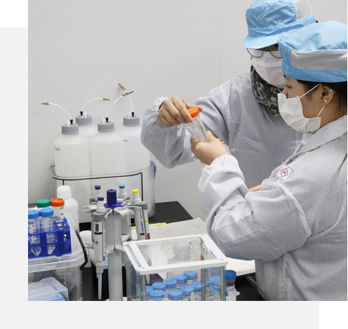
Contamination in the semiconductor process is metallic, organic, and ionic contamination. Depending on the causes of contamination, it can be distinguished by origin, equipment origin, and process origin. In the past, the management of such contamination has been used to analyze the contamination of materials or wafers off-line when the cause of the yield deterioration has not been found.
The NvisANA's company affiliated research institute has developed the world's first fully automated in-line pollution monitoring equipment to provide wafer management solutions to semiconductor companies for metal contamination. We are making efforts to become a Contamination Monitoring Total Solution Provider, which provides technology to device manufacturers as well as semiconductor ecosystems.