As the device node enters into 20nm era, the effect of non-visual defects, such as metallic and non-metallic contamination,
on the device performance is getting more and more significant and cannot be neglected anymore.
And the non-visual defect control will be crucial to yield management of under 20nm devices.
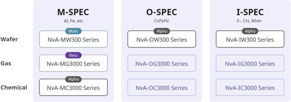
Our M-SPEC, O-SPEC and I-SPEC provides you with total solution of metallic, organic and ionic contamination monitoring for gases,
chemicals and wafers in the semiconductor ecosystem, respectively.
on the device performance is getting more and more significant and cannot be neglected anymore.
And the non-visual defect control will be crucial to yield management of under 20nm devices.
Our M-SPEC, O-SPEC and I-SPEC provides you with total solution of metallic, organic and ionic contamination monitoring for gases,
chemicals and wafers in the semiconductor ecosystem, respectively.